
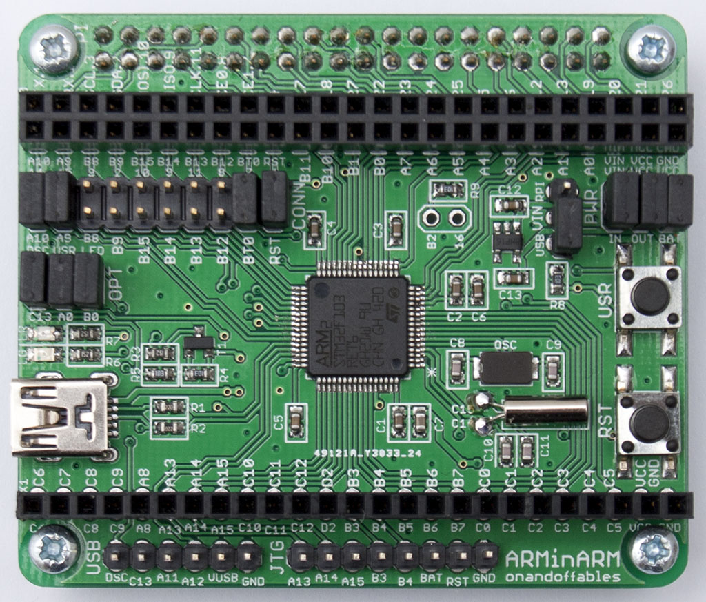
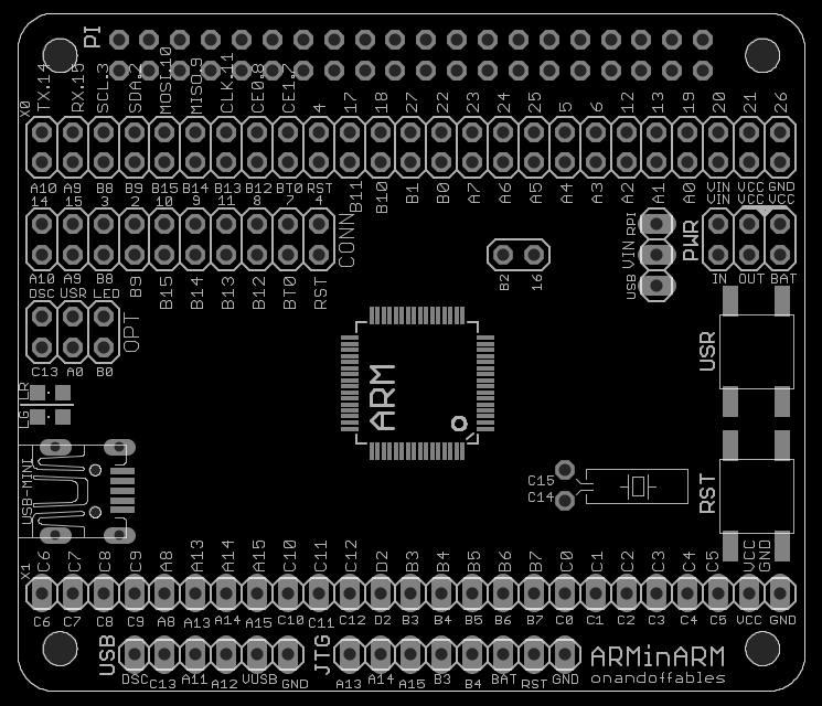
Pinout
The female headers (X0 and X1) on the board are connected to the pins of the STM32 and GPIO pins on the Raspberry Pi. X0 is the top 2x25 female header, and X1 is the bottom 1x25 female header.
The board also contains dual row male headers to choose power options, and directly connect suitable pins from the STM32 to the Raspberry Pi.
All GPIO is 3.3 Volt logic, but a lot of the STM32 GPIO pins are 5 Volt tolerant. Look for the red 'no' or the green 'yes' in the '5V' column of the table below to see if a particular pin is 5 volt tolerant or not.
X0 Header (RPI)All of the Raspberry Pi GPIO pins are broken out to this header (except for GPIO16, see BOOT1 Header). For a detailed description of these pins, see: http://elinux.org/RPi_BCM2835_GPIOs 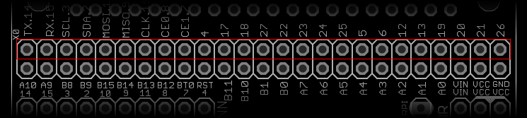 | |||||
| Pin | Type | 5V | Pull | Default | Remap |
|---|---|---|---|---|---|
| TX.14 | RPI | NO | low | GPIO14 | USART_TXD |
| RX.15 | RPI | NO | low | GPIO15 | USART_RXD |
| SCL.3 | RPI | NO | high | GPIO3 | I2C1_SCL |
| SDA.2 | RPI | NO | high | GPIO2 | I2C1_SDA |
| MOSI.10 | RPI | NO | low | GPIO10 | SPI0_MOSI |
| MISO.9 | RPI | NO | low | GPIO9 | SPI0_MISO |
| SCK.11 | RPI | NO | low | GPIO11 | SPI0_SCK |
| CE0.8 | RPI | NO | high | GPIO8 | SPI0_CE0 |
| CE1.7 | RPI | NO | high | GPIO7 | SPI0_CE1 |
| GPIO4 | RPI | NO | high | GPIO4 | GPCLK0 |
| GPIO17 | RPI | NO | low | GPIO17 | GPIO_GEN0 |
| GPIO18 | RPI | NO | low | GPIO18 | GPIO_GEN1 |
| GPIO27 | RPI | NO | low | GPIO27 | GPIO_GEN2 |
| GPIO22 | RPI | NO | low | GPIO22 | GPIO_GEN3 |
| GPIO23 | RPI | NO | low | GPIO23 | GPIO_GEN4 |
| GPIO24 | RPI | NO | low | GPIO24 | GPIO_GEN5 |
| GPIO25 | RPI | NO | low | GPIO25 | GPIO_GEN6 |
| GPIO5 | RPI | NO | high | GPIO5 | CAM_CLK |
| GPIO6 | RPI | NO | high | GPIO6 | LAN_RUN |
| GPIO12 | RPI | NO | low | GPIO12 | PWM0 |
| GPIO19 | RPI | NO | low | GPIO19 | - |
| GPIO20 | RPI | NO | low | GPIO20 | - |
| GPIO21 | RPI | NO | low | GPIO21 | GPCLK1 |
| GPIO26 | RPI | NO | low | GPIO26 | - |
X0 Header (STM32)Part of the STM32 GPIO pins are broken out on this header. Some of them are probably connected to Raspberry Pi pins to program the STM32 (see CONN header). Don't put 5V on STM32 pins that are also connected to the Raspberry Pi, even though they're 5V tolerant. The corresponding Raspberry Pi pins aren't so tolerant and you'll break stuff.  | |||||
| Pin | Type | 5V | Startup | Default | Remap |
| PA10 | I/O | YES | PA10 | USART1_RX/TIM1_CH3 | |
| PA9 | I/O | YES | PA9 | USART1_TX/TIM1_CH2 | |
| PB8 | I/O | YES | PB8 | TIM4_CH3/SDIO_D4 | I2C1_SCL/CAN_RX |
| PB9 | I/O | YES | PB9 | TIM4_CH4/SDIO_D5 | I2C1_SDA/CAN_TX |
| PB15 | I/O | YES | PB15 | SPI2_MOSI/I2S2_SD/TIM1_CH3N | |
| PB14 | I/O | YES | PB14 | SPI2_MISO/TIM1_CH2N/USART3_RTS | |
| PB13 | I/O | YES | PB13 | SPI2_SCK/I2S2_CK/USART3_CTS/TIM1_CH1N | |
| PB12 | I/O | YES | PB12 | SPI2_NSS/I2S2_WS/I2C2_SMBA/USART3_CK/TIM1_BKIN | |
| BOOT0 | I | NO | BOOT0 | ||
| NRST | I/O | NO | NRST | ||
| PB11 | I/O | YES | PB11 | I2C2_SDA/USART3_RX | TIM2_CH4 |
| PB10 | I/O | YES | PB10 | I2C2_SCL/USART3_TX | TIM2_CH3 |
| PB1 | I/O | NO | PB1 | ADC12_IN9/TIM3_CH4/TIM8_CH3N | TIM1_CH3N |
| PB0 | I/O | NO | PB0 | ADC12_IN8/TIM3_CH3/TIM8_CH2N | TIM1_CH2N |
| PA7 | I/O | NO | PA7 | SPI1_MOSI/TIM8_CH1N/ADC12_IN7/TIM3_CH2 | TIM1_CH1N |
| PA6 | I/O | NO | PA6 | SPI1_MISO/TIM8_BKIN/ADC12_IN6/TIM3_CH1 | TIM1_BKIN |
| PA5 | I/O | NO | PA5 | SPI1_SCK/DAC_OUT2/ADC12_IN5 | |
| PA4 | I/O | NO | PA4 | SPI1_NSS/USART2_CK/DAC_OUT1/ADC12_IN4 | |
| PA3 | I/O | NO | PA3 | USART2_RX/TIM5_CH4/ADC123_IN3/TIM2_CH4 | |
| PA2 | I/O | NO | PA2 | USART2_TX/TIM5_CH3/ADC123_IN2/TIM2_CH3 | |
| PA1 | I/O | NO | PA1 | USART2_RTS/ADC123_IN1/TIM5_CH2/TIM2_CH2 | |
| PA0 | I/O | NO | PA0 | WKUP/USART2_CTS/ADC123_IN0/TIM2_CH1_ETR/TIM5_CH1/TIM8_ETR | |
| VIN | PWR | YES | - | External (PWR) | 5V from RPI or USB |
| VCC | PWR | NO | VCC (3V3) | ||
| GND | PWR | NO | GND (VSS) | ||
CONN HeaderThe CONN header is a 1:1 duplicate of the first 2x10 pins of header X0. On this header, you can make direct connections from the STM32 to the RPI (USART, I2C, SPI, BOOT0, RST) using jumpers. To program the STM32 using the bootloader, put jumpers on PA10/GPIO14, PA9/GPIO15, BOOT0/GPIO7(CE1) and NRST/GPIO4. In other words, at least 4 jumpers: 2 jumpers on the far left, and 2 jumpers on the far right of the CONN header. After programming is done you can do with the pins as you please (see X0 header). It might make sense to just leave the jumpers on there though. You can use the UART connection to communicate between the STM32 and the Raspberry Pi. You'll probably want to always keep BOOT0/GPIO7 and NRST/GPIO4 pins jumpered too, because they're not extremely useful for other things. They're available on the X0 header if you do need them. For faster communication than UART, jumper the appropriate pins and use the STM32 as an I2C or SPI slave (the Raspberry Pi can only be master). 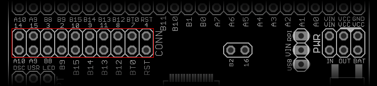 | |||||
| Pin | Type | 5V | Function | With Jumper | Info |
| A10-IO14 | I/O | NO | UART | Connects STM32 RX (PA10) to RPI TX (GPIO14) | jumper for bootloader |
| A9-IO15 | I/O | NO | UART | Connects STM32 TX (PA9) to RPI RX (GPIO15) | jumper for bootloader |
| B8-IO3 | I/O | NO | I2C | Connects STM32 SCL (PB8) to RPI SCL (GPIO3) | |
| B9-IO2 | I/O | NO | I2C | Connects STM32 SDA (PB8) to RPI SDA (GPIO2) | |
| B15-IO10 | I/O | NO | SPI | Connects STM32 MOSI (PB15) to RPI MOSI (GPIO10) | |
| B14-IO9 | I/O | NO | SPI | Connects STM32 MISO (PB14) to RPI MISO (GPIO9) | |
| B13-IO11 | I/O | NO | SPI | Connects STM32 SCK (PB13) to RPI SCK (GPIO11) | |
| B12-IO8 | I/O | NO | SPI | Connects STM32 NSS (PB12) to RPI CE0 (GPIO8) | |
| BT0-IO7 | I/O | NO | BOOT0 | Connects STM32 BOOT0 (BOOT0) to RPI CE1 (GPIO7) | jumper for bootloader |
| RST-IO4 | I/O | NO | NRST | Connects STM32 NRST (NRST) to RPI GPIO4 | jumper for bootloader |
BOOT1 HeaderBoth PB2/BOOT1 (STM32) and GPIO16 (RPI) are broken out to this header. Optionally solder a 1x2 male pinheader here and install a jumper to upload firmware to the STM32 SRAM section (or pull BOOT1 high some other way). The default (without a jumper) is to upload to STM32 Flash memory. One reason to upload your firmware to SRAM might be to save wear on the Flash memory. The Flash memory is rated for anywhere between 10 kilocycles to 100 kilocycles rewrites. If you think about that for a moment, you may come to the conclusion it's not worth the hassle. It's here if you need it. PB2/BOOT1 is pulled low with a 10K resistor. 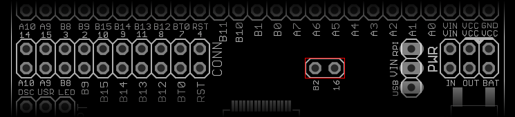 | |||||
| Pin | Type | 5V | Startup | Default | Remap |
| PB2 | I/O | YES | PB2/BOOT1 | ||
| GPIO16 | RPI | NO | low | GPIO16 | STATUS_LED_N |
VIN HeaderPut a jumper on either RPI/VIN or USB/VIN, depending on where you want the 5V power from. If you supply power yourself to VIN (max. 5V), leave off the RPI or USB jumper connecting to VIN (seriously!). If you're backpowering 5V to the Raspberry Pi through VIN or otherwise, please take the necessary precautions. To use the ARMinARM board on the Raspberry Pi, you'll want a jumper connecting the RPI to the VIN pin. To use the board standalone (powered from USB), move the jumper to the USB/VIN pin combination. 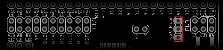 | |||||
| Pin | Type | 5V | Startup | Default | With Jumper |
| RPI | PWR | YES | - | Power from RPI (5V) | 5V from RPI |
| VIN | PWR | YES | - | External (PWR) | 5V from RPI or USB |
| USB | PWR | YES | - | Power from USB (5V) | 5V from USB |
PWR HeaderMore options to decide how you want to power the board. You'll probably want all 3 jumpers on here (IN/VIN, OUT/VCC, BAT/VCC). If you're not using a battery, connecting VBAT to VCC is highly recommended. It keeps the RTC running and remembers the content of backup registers. You can bypass the onboard 3.3V voltage regulator completely by leaving off the IN/VIN and OUT/VCC jumpers (in that case, power VCC with your own 3.3V). Never connect more than 5 volt to the input of the voltage regulator! 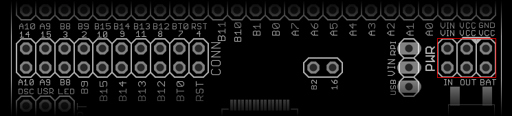 | |||||
| Pin | Type | 5V | Startup | Default | - |
| IN | PWR | YES | - | Connects Voltage Regulator in to VIN | Max. 5 Volt |
| OUT | PWR | NO | - | Connects Voltage Regulator out to VCC (3V3) | |
| VBAT | PWR | NO | - | Connect to VCC | |
OPT HeaderThe OPT header contains the pins that define the ARMinARM board. Jumper PC13 to the USB Disconnect circuitry. You'll need it if you want to program the STM32 as a USB device. Jumper the USR button to PA0. The USR button is also connected to the BOOT0 pin, and is therefore pulled down to GND. To use PA0 as an analog input (and read values other than 0) you'll want to disconnect it from the USR button. Note that when you disconnect PA0 from the USR button, it is still possible to use the buttons USR and RST to put the STM32 into bootloader mode. Jumper the LED pin to PB0 to use the onboard LED. PB0 is a PWM capable pin. If you want to use PB0 for anything else and the LED annoys you, disconnect it. 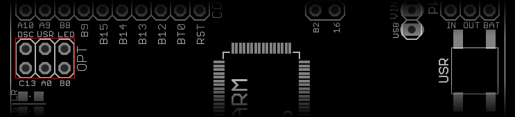 | |||||
| Pins | Type | 5V | Startup | With Jumper | - |
| DSC-PC13 | I/O | NO | - | Connects DISCONNECT circuitry to PC13 | |
| USR-PA0 | I/O | NO | - | Connects USR button to PA0 | |
| LED-PB0 | I/O | NO | - | Connects onboard red LED to PB0 | |
XTAL Header (32.768KHz oscillator)Footprint to solder a 32.768KHz crystal. Connected to PC14 and PC15 on the STM32. A crystal here does a better job keeping time and date than the internal oscillator. If you want to use these pins for anything else, it's just a 1x2 pinheader footprint that aligns to the 0.1" grid. You can break them out to a prototyping board. Be careful though. They can't drive loads, so you can't blink LEDs with them. 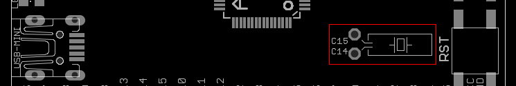 | |||||
| Pin | Type | 5V | Startup | Default | Remap |
| PC14 | I/O | NO | PC14 | OSC32_IN | |
| PC15 | I/O | NO | PC15 | OSC32_OUT | |
X1 Header (STM32)(Most of) the rest of the STM32 GPIO pins are broken out on this header. 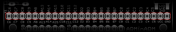 | |||||
| Pin | Type | 5V | Startup | Default | Remap |
| PC6 | I/O | YES | PC6 | I2S2_MCK/TIM8_CH1/SDIO_D6 | TIM3_CH1 |
| PC7 | I/O | YES | PC7 | I2S3_MCK/TIM8_CH2/SDIO_D7 | TIM3_CH2 |
| PC8 | I/O | YES | PC8 | TIM8_CH3/SDIO_D0 | TIM3_CH3 |
| PC9 | I/O | YES | PC9 | TIM8_CH4/SDIO_D1 | TIM3_CH4 |
| PA8 | I/O | YES | PA8 | USART1_CK/TIM1_CH1/MCO | |
| PA13 | I/O | YES | JTMS-SWDIO | PA13 | |
| PA14 | I/O | YES | JTCK-SWCLK | PA14 | |
| PA15 | I/O | YES | JTDI | SPI3_NSS/I2S3_WS | TIM2_CH1_ETR/PA15/SPI1_NSS |
| PC10 | I/O | YES | PC10 | UART4_TX/SDIO_D2 | USART3_TX |
| PC11 | I/O | YES | PC11 | UART4_RX/SDIO_D3 | USART3_RX |
| PC12 | I/O | YES | PC12 | UART5_TX/SDIO_CK | USART3_CK |
| PD2 | I/O | YES | PD2 | TIM3_ETR/UART5_RX/SDIO_CMD | |
| PB3 | I/O | YES | JTDO | SPI3_SCK/I2S3_CK | PB3/TRACESWO/TIM2_CH2/SPI1_SCK |
| PB4 | I/O | YES | NJTRST | SPI3_MISO | PB4/TIM3_CH1/SPI1_MISO |
| PB5 | I/O | NO | PB5 | I2C1_SMBA/SPI3_MOSI/I2S3_SD | TIM3_CH2/SPI1_MOSI |
| PB6 | I/O | YES | PB6 | I2C1_SCL/TIM4_CH1 | USART1_TX |
| PB7 | I/O | YES | PB7 | I2C1_SDA/FSMC_NADV/TIM4_CH2 | USART1_RX |
| PC0 | I/O | NO | PC0 | ADC123_IN10 | |
| PC1 | I/O | NO | PC1 | ADC123_IN11 | |
| PC2 | I/O | NO | PC2 | ADC123_IN12 | |
| PC3 | I/O | NO | PC3 | ADC123_IN13 | |
| PC4 | I/O | NO | PC4 | ADC12_IN14 | |
| PC5 | I/O | NO | PC5 | ADC12_IN15 | |
| VCC | PWR | NO | VCC (3V3) | ||
| GND | PWR | NO | GND (VSS) | ||
USB HeaderThe USB header contains 'everything USB'. Mainly to break out pins PA11 and PA12, the D+ and D- (USB data) pins of the STM32. They're here if you need them for anything else (and having PC13, VUSB and a GND there is of course handy as well). In emergencies, another STM32 GPIO than PC13 can be routed to the DSC (USB Disconnect circuitry) pin here if you want to make the ARMinARM board hardware compatible with other boards (without recompiling their firmware). Or other unforeseen situations you might encounter. It's here if you're looking for it. 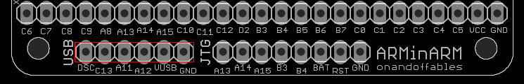 | |||||
| Pin | Type | 5V | Startup | Default | Remap |
| DSC | I/O | NO | - | DISCONNECT circuitry | |
| PC13 | I/O | NO | PC13 | TAMPER-RTC | USB Disconnect |
| PA11 | I/O | YES | PA11 | USART1_CTS/USBDM/CAN_RX/TIM1_CH4 | |
| PA12 | I/O | YES | PA12 | USART1_RTS/USBDP/CAN_TX/TIM1_ETR | |
| VUSB | PWR | YES | VUSB (5V) | ||
| GND | PWR | NO | GND (VSS) | ||
JTAG HeaderMost of the pins on this header are also on the X1 header right above it. They're pins used for SWD or JTAG in all its incarnations and pin standards. Solder male pins on here and you can easily probe them from the outside without removing any addon boards (caps). Note that BAT is actually VCC (3.3V) if you have the BAT/VCC jumper on the PWR header. If you want to use a battery, you want that jumper removed. You can connect the battery either on this pin now, or on the BAT pin on the PWR header. In situations where the RST button is hard to reach, you can temporarily short the 2 right-most pins of this header to reset the board. They're NRST and GND. Think 'conductive material'. Like a paperclip, screwdriver, keys etc. 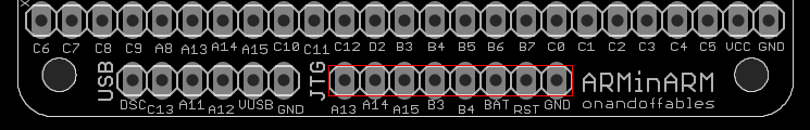 | |||||
| Pin | Type | 5V | Startup | Default | Remap |
| PA13 | I/O | YES | JTMS-SWDIO | PA13 | |
| PA14 | I/O | YES | JTCK-SWCLK | PA14 | |
| PA15 | I/O | YES | JTDI | SPI3_NSS/I2S3_WS | TIM2_CH1_ETR/PA15/SPI1_NSS |
| PB3 | I/O | YES | JTDO | SPI3_SCK/I2S3_CK | PB3/TRACESWO/TIM2_CH2/SPI1_SCK |
| PB4 | I/O | YES | NJTRST | SPI3_MISO | PB4/TIM3_CH1/SPI1_MISO |
| VBAT | PWR | NO | - | Connect to VCC | |
| NRST | I/O | NO | NRST | ||
| GND | PWR | NO | GND (VSS) | ||